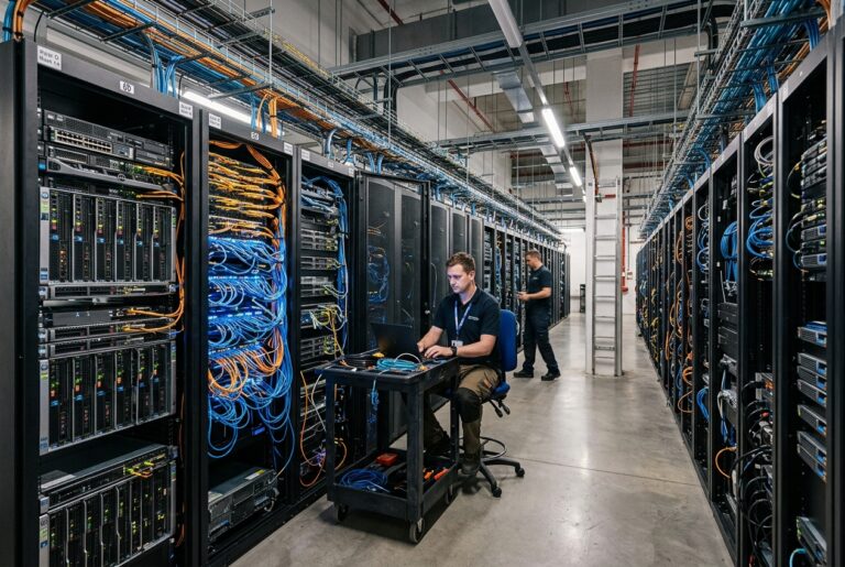
The global semiconductor industry, currently led by giants like Nvidia, may be hurtling toward an inevitable physical plateau. Huawei’s chief semiconductor scientist recently voiced concerns that the current focus on ultra-fine manufacturing processes and High Bandwidth Memory (HBM) is nearing its absolute limit. This warning suggests that the aggressive pursuit of miniaturization might soon yield diminishing returns for the world’s most advanced AI hardware.
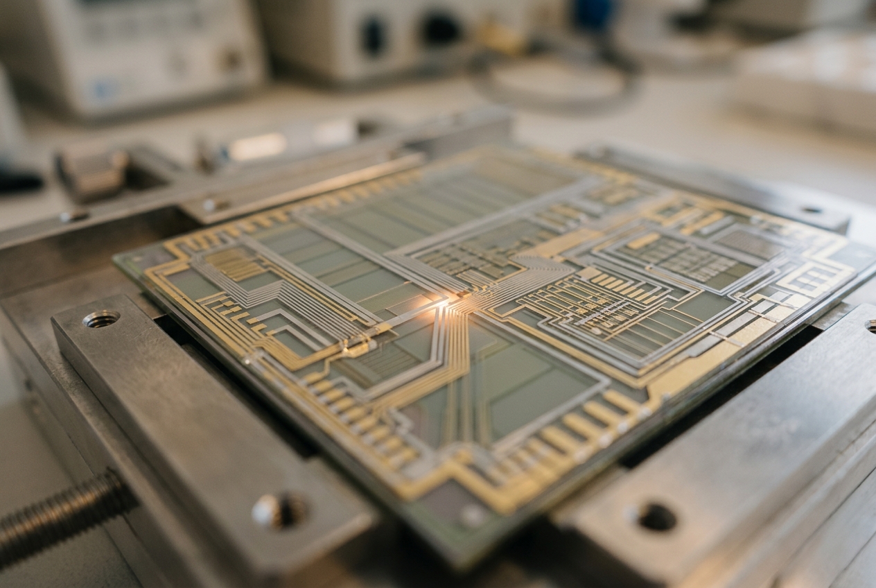
According to the report, the traditional method of boosting performance by shrinking transistor sizes—often referred to as Moore’s Law—is becoming increasingly difficult and prohibitively expensive. As chips reach the 2nm or 1nm threshold, quantum interference and heat dissipation issues begin to outweigh the performance gains. This physical reality poses a significant threat to the roadmap of companies currently dominating the AI infrastructure market.
Shifting the Focus: From Brute Force to Efficiency
While the rest of the world remains obsessed with nanometer-scale miniaturization, Huawei is reportedly pivoting its strategy. The Chinese tech giant is prioritizing data transmission efficiency over raw transistor count. This approach aims to solve the “memory wall” problem, where the speed of the processor far outpaces the speed at which data can be moved across the system.
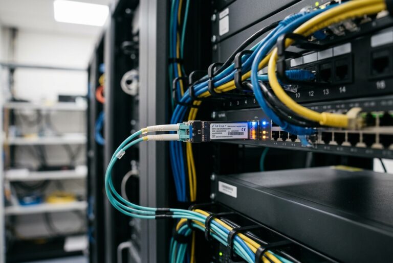
By focusing on proprietary technologies like ‘Ta’, Huawei seeks to optimize how data flows within and between chips. This methodology suggests that the next leap in AI performance will not come from smaller chips, but from smarter interconnectivity and reduced latency in data processing pipelines. This represents a fundamental shift in how high-performance computing is architected.
Geopolitical Pressure as a Catalyst for Innovation
The context of these remarks cannot be ignored. Under heavy U.S. trade sanctions, Huawei has been forced to innovate without access to the latest extreme ultraviolet (EUV) lithography equipment. This necessity has birthed a different school of thought, one that views architectural optimization as the primary driver for future growth rather than mere hardware scaling.
- Optimization of chip-to-chip communication protocols
- Enhanced software-hardware integration for AI workloads
- Reduced reliance on ultra-fine lithography through modular design
- Focus on energy-efficient data throughput
Ultimately, the semiconductor landscape is at a crossroads. If Huawei’s predictions hold true, the industry’s reliance on HBM-centric performance will eventually face a ceiling. The winner of the next decade may not be the company with the smallest transistors, but the one that manages data most effectively across distributed systems. As physical limits approach, the battle for AI supremacy is moving from the foundry to the architecture lab.
작성자 소개